- 您现在的位置:买卖IC网 > Sheet目录2003 > LTC1402IGN#TRPBF (Linear Technology)IC ADC 12BIT 2.2MSPS SHDN 16SSOP
2
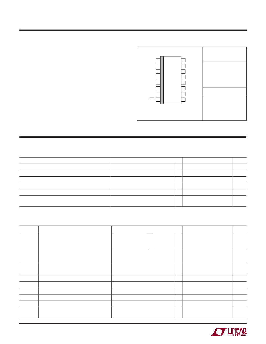
LTC1402
TOP VIEW
GN PACKAGE
16-LEAD NARROW PLASTIC SSOP
1
2
3
4
5
6
7
8
16
15
14
13
12
11
10
9
AVDD
AGND1
AIN
+
AIN
–
VREF
AGND2
GAIN
BIP/UNI
CONV
SCK
VSS
DGND
DVDD
0VDD
DOUT
OGND
PACKAGE/ORDER INFORMATION
W
U
ABSOLUTE MAXIMUM RATINGS
W
WW
U
AVDD = DVDD = OVDD = VDD (Notes 1, 2)
Supply Voltage (VDD) ................................................. 6V
Negative Supply Voltage (VSS) ............................... – 6V
Total Supply Voltage (VDD to VSS) .......................... 12V
Analog Input Voltage
(Note 3) .......................... (VSS – 0.3V) to (VDD + 0.3V)
Digital Input Voltage
(Note 4) .......................... (VSS – 0.3V) to (VDD + 0.3V)
Digital Output Voltage ......... (VSS – 0.3V) to (VDD + 0.3V)
Power Dissipation .............................................. 250mW
Operation Temperature Range
LTC1402C ............................................... 0
°C to 70°C
LTC1402I ............................................ – 40
°C to 85°C
Storage Temperature Range ................. – 65
°C to 150°C
Lead Temperature (Soldering, 10 sec).................. 300
°C
ORDER PART
NUMBER
GN PART MARKING
1402
1402I
Consult factory for Military grade parts.
LTC1402CGN
LTC1402IGN
TJMAX = 125°C, θJA = 150°C/ W
CONVERTER CHARACTERISTICS
U
The q denotes the specifications which apply over the full operating
temperature range, otherwise specifications are at TA = 25°C. With internal reference (Note 5).
PARAMETER
CONDITIONS
MIN
TYP
MAX
UNITS
Resolution (No Missing Codes)
q
12
Bits
Integral Linearity Error
(Note 6)
q
±0.35
±1LSB
Differential Linearity
(Note 6)
q
±0.25
±1LSB
Offset Error
(Note 6)
q
±2
±10
LSB
Full-Scale Error
(Note 6)
q
±10
±15
LSB
Full-Scale Tempco
Internal Reference (Note 6)
±15
ppm/
°C
External Reference
±1
ppm/
°C
The q denotes the specifications which apply over the full operating temperature range,
otherwise specifications are at TA = 25°C. (Note 5)
SYMBOL
PARAMETER
CONDITIONS
MIN
TYP
MAX
UNITS
VIN
Analog Differential Input Range (Notes 3, 11)
Bipolar Mode with BIP/UNI High
q
±2.048
V
4.75V
≤ VDD ≤ 5.25V
– 5.25V
≤ VSS ≤ –4.75V
Unipolar Mode with BIP/UNI Low
q
0 to 4.096
V
4.75V
≤ VDD ≤ 5.25V
– 5.25V
≤ VSS ≤ 0V
VCM
Analog Common Mode + Differential
Dual
±5V Supply
–2.5 to 5
V
Input Range (Note 12)
Single 5V Supply
0 to 5
V
IIN
Analog Input Leakage Current
q
1
A
CIN
Analog Input Capacitance
10
pF
tACQ
Sample-and-Hold Acquisition Time
(Note 9)
q
57
ns
tAP
Sample-and-Hold Aperture Delay Time
2.6
ns
tJITTER
Sample-and-Hold Aperture Delay Time Jitter
1
ps
CMRR
Analog Input Common Mode Rejection Ratio
fIN = 1MHz, VIN = 2V to – 2V
– 62
dB
fIN = 100MHz, VIN = 2V to – 2V
– 24
dB
A ALOG I PUT
U
发布紧急采购,3分钟左右您将得到回复。
相关PDF资料
LTC1403AHMSE#TRPBF
IC ADC 14BIT 2.8MSPS DIFF 10MSOP
LTC1403AIMSE-1#TRPBF
IC ADC 14BIT 2.8MSPS DIFF 10MSOP
LTC1404IS8#TRPBF
IC A/D CONV 12BIT W/SHTDN 8-SOIC
LTC1405IGN#TRPBF
IC ADC 12BIT 5MSPS SAMPLE 28SSOP
LTC1406IGN#TRPBF
IC A/D CONV 8BIT SAMPLING 24SSOP
LTC1407AHMSE#PBF
IC ADC 14BIT 3MSPS 10-MSOP
LTC1407AIMSE-1#TRPBF
IC ADC 14BIT 3MSPS SAMPLE 10MSOP
LTC1408IUH-12#TRPBF
IC ADC 12BIT 600KSPS 32-QFN
相关代理商/技术参数
LTC1403ACMSE
功能描述:IC ADC 14BIT 2.8MSPS DIFF 10MSOP RoHS:否 类别:集成电路 (IC) >> 数据采集 - 模数转换器 系列:- 标准包装:1,000 系列:- 位数:16 采样率(每秒):45k 数据接口:串行 转换器数目:2 功率耗散(最大):315mW 电压电源:模拟和数字 工作温度:0°C ~ 70°C 安装类型:表面贴装 封装/外壳:28-SOIC(0.295",7.50mm 宽) 供应商设备封装:28-SOIC W 包装:带卷 (TR) 输入数目和类型:2 个单端,单极
LTC1403ACMSE#PBF
功能描述:IC ADC 14BIT 2.8MSPS 10-MSOP RoHS:是 类别:集成电路 (IC) >> 数据采集 - 模数转换器 系列:- 标准包装:1 系列:microPOWER™ 位数:8 采样率(每秒):1M 数据接口:串行,SPI? 转换器数目:1 功率耗散(最大):- 电压电源:模拟和数字 工作温度:-40°C ~ 125°C 安装类型:表面贴装 封装/外壳:24-VFQFN 裸露焊盘 供应商设备封装:24-VQFN 裸露焊盘(4x4) 包装:Digi-Reel® 输入数目和类型:8 个单端,单极 产品目录页面:892 (CN2011-ZH PDF) 其它名称:296-25851-6
LTC1403ACMSE#PBF
制造商:Linear Technology 功能描述:ADC, 14BIT, 2.8MSPS, MSOP-10
LTC1403ACMSE#TR
功能描述:IC ADC 14BIT 2.8MSPS DIFF 10MSOP RoHS:否 类别:集成电路 (IC) >> 数据采集 - 模数转换器 系列:- 标准包装:1,000 系列:- 位数:16 采样率(每秒):45k 数据接口:串行 转换器数目:2 功率耗散(最大):315mW 电压电源:模拟和数字 工作温度:0°C ~ 70°C 安装类型:表面贴装 封装/外壳:28-SOIC(0.295",7.50mm 宽) 供应商设备封装:28-SOIC W 包装:带卷 (TR) 输入数目和类型:2 个单端,单极
LTC1403ACMSE#TRPBF
功能描述:IC ADC 14BIT 2.8MSPS DIFF 10MSOP RoHS:是 类别:集成电路 (IC) >> 数据采集 - 模数转换器 系列:- 标准包装:1,000 系列:- 位数:16 采样率(每秒):45k 数据接口:串行 转换器数目:2 功率耗散(最大):315mW 电压电源:模拟和数字 工作温度:0°C ~ 70°C 安装类型:表面贴装 封装/外壳:28-SOIC(0.295",7.50mm 宽) 供应商设备封装:28-SOIC W 包装:带卷 (TR) 输入数目和类型:2 个单端,单极
LTC1403ACMSE-1
功能描述:IC ADC 14BIT 2.8MSPS DIFF 10MSOP RoHS:否 类别:集成电路 (IC) >> 数据采集 - 模数转换器 系列:- 标准包装:1,000 系列:- 位数:16 采样率(每秒):45k 数据接口:串行 转换器数目:2 功率耗散(最大):315mW 电压电源:模拟和数字 工作温度:0°C ~ 70°C 安装类型:表面贴装 封装/外壳:28-SOIC(0.295",7.50mm 宽) 供应商设备封装:28-SOIC W 包装:带卷 (TR) 输入数目和类型:2 个单端,单极
LTC1403ACMSE-1#PBF
功能描述:IC ADC 14BIT 2.8MSPS 10-MSOP RoHS:是 类别:集成电路 (IC) >> 数据采集 - 模数转换器 系列:- 标准包装:1 系列:microPOWER™ 位数:8 采样率(每秒):1M 数据接口:串行,SPI? 转换器数目:1 功率耗散(最大):- 电压电源:模拟和数字 工作温度:-40°C ~ 125°C 安装类型:表面贴装 封装/外壳:24-VFQFN 裸露焊盘 供应商设备封装:24-VQFN 裸露焊盘(4x4) 包装:Digi-Reel® 输入数目和类型:8 个单端,单极 产品目录页面:892 (CN2011-ZH PDF) 其它名称:296-25851-6
LTC1403ACMSE-1#TR
功能描述:IC ADC 14BIT 2.8MSPS DIFF 10MSOP RoHS:否 类别:集成电路 (IC) >> 数据采集 - 模数转换器 系列:- 标准包装:1,000 系列:- 位数:16 采样率(每秒):45k 数据接口:串行 转换器数目:2 功率耗散(最大):315mW 电压电源:模拟和数字 工作温度:0°C ~ 70°C 安装类型:表面贴装 封装/外壳:28-SOIC(0.295",7.50mm 宽) 供应商设备封装:28-SOIC W 包装:带卷 (TR) 输入数目和类型:2 个单端,单极